

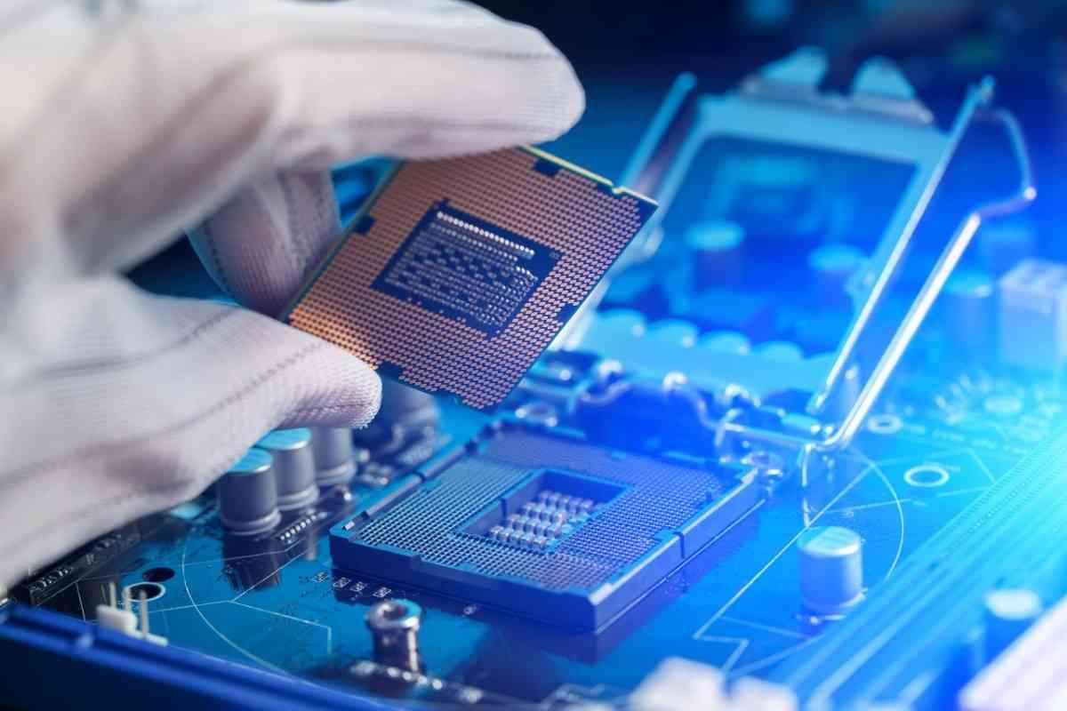
Embedded Hardware Design Company in San Jose, CA: Eliminating Cross-Talk in High-Speed Clocks
In the high-frequency computing systems engineered across Silicon Valley, clock distribution networks function as the absolute heartbeat of physical computing platforms. As edge computing architectures, high-density AI accelerators, and complex industrial IoT systems move into high-volume Big Production runs, clock frequencies are climbing into the gigahertz range, accompanied by sub-nanosecond signal rise times ($t_r$). At these speeds, traditional printed circuit board (PCB) traces can no longer be treated as simple visual connections; they act as transmission lines governed by complex electromagnetic fields.
When signal rise times are incredibly fast, the primary engineering challenge shifts from basic schematic wiring to maintaining strict Signal Integrity Standards. The most destructive problem plaguing high-density multilayer configurations is Cross-Talk—the unwanted electromagnetic coupling between a high-speed clock trace (the aggressor) and an adjacent sensitive data track (the victim). Unchecked cross-talk introduces timing jitter, clock edge distortion, and data corruption, which can quickly ruin an entire production fleet.
At Jenex Technovation Pvt. Ltd., we operate as a premier, full-cycle Embedded Hardware Design Company in San Jose, CA. We manage the critical Hardware-Software Bridge by enforcing precise physical routing models and rigorous board-level physics to eliminate cross-talk in high-speed timing distribution networks.
The Physics of Interference: Why Standard Board Layout Habits Fail at High Frequencies
Many general PCB layout bureaus approach trace routing using basic geometric routing paths without simulating dynamic electromagnetic interactions. At low frequencies, these simple assumptions hold true. However, when high-speed clock lines feature rapid edge transitions, they generate intense, moving electric ($E$) and magnetic ($H$) fields that radiate outward.
This energy transfers to nearby tracks through capacitive coupling (due to parasitic mutual capacitance, $C_m$) and inductive coupling (due to mutual inductance, $L_m$). If your board layout parameters fail to actively isolate these energy fields, the resulting noise overrides your logic thresholds, leading to unpredictable system errors in the field.
To protect your complex high-speed timing networks from signal distortion, Jenex Technovation Pvt. Ltd. implements a rigorous engineering roadmap across these seven core layout pillars:
1. Enforcing the 3W Separation Rule and Guard Trace Architectures
Placing high-speed clock lines right next to parallel data routing tracks allows mutual capacitance and inductance to quickly corrupt your system signals.
-
The Jenex Standard: We apply strict Board Layout Metrics to establish physical isolation. We enforce a mandatory 3W Spacing Rule, ensuring the center-to-center distance between a high-speed clock line and any adjacent track is at least three times the width ($W$) of the clock line trace. For critical differential clock lines, we insert custom coplanar ground guard traces with continuous vias connected straight to the internal ground layers, creating a solid electromagnetic wall around the clock path.
2. Embedded Stripline Routing Configurations in Symmetric Stack-Ups
Routing high-frequency clock signals across the open top or bottom surfaces of a PCB ($microstrip\ lines$) allows electromagnetic energy to radiate freely, creating severe cross-talk and failing FCC emissions testing.
-
The Jenex Standard: We route high-speed clock lines exclusively as Embedded Striplines on internal PCB layers. By placing the clock line between two solid, continuous copper reference ground planes separated by precise dielectric materials, we trap the electromagnetic fields entirely within that layer. This shielding cuts forward and backward cross-talk by up to 90%.
  Layer 1: Solid Copper Ground Plane (0V Reference)
  ──────────────────────────────────────────────────────────
  Dielectric Core Material (Prepreg)
       [ Victim Trace ]   ◄── 3W Distance ──►   [ Clock Trace (Aggressor) ]
  Dielectric Core Material (Prepreg)
  ──────────────────────────────────────────────────────────
  Layer 2: Solid Copper Ground Plane (0V Reference)

  ▲ Internal Stripline Architecture isolates electromagnetic radiation between solid ground shields.
3. Precision Controlled Impedance Matching Geometry
Any physical mismatch along a high-speed clock line trace—such as sudden width shifts, sharp track bends, or unplanned test points—causes signal reflection waves that amplify cross-talk noise.
-
The Jenex Standard: We design our high-frequency tracks to meet exact $50\,\Omega$ single-ended and $100\,\Omega$ differential impedance values. We use continuous, smooth curves rather than sharp $90^\circ$ angles and use advanced time-domain reflectometry ($TDR$) simulations to verify that the trace width matches the dielectric material properties perfectly along the entire routing path.
4. Minimizing Layer Transitions to Maintain Clean Return Current Paths
Forcing a high-frequency clock trace to hop between multiple board layers through vertical vias without a clear adjacent ground path creates massive ground loops, causing the signal return current to wander and generate cross-talk noise across nearby layers.
-
The Jenex Standard: We minimize layer transitions for high-frequency timing paths, keeping them on a single internal layer from source to destination. If a layer change is absolutely required, we place dedicated GND Stitching Vias right next to the signal via. This structure provides an immediate, low-impedance path for the return current, preventing loop radiation.
5. Advanced Power Distribution Network (PDN) Decoupling Topology
High-speed switching currents within clock driver chips can cause sudden voltage drops on internal power rails, introducing phase jitter and noise into your timing system.
-
The Jenex Standard: We design robust, low-impedance power networks within our Embedded Hardware Solutions. We position low-inductance ceramic decoupling capacitors right against the power pins of your clock generation chips, utilizing short, wide traces to eliminate parasitic inductance and maintain clean, stable power profiles.
6. Dynamic Co-Design for High-Performance Edge AI Arrays (TinyML)
Deploying advanced neural network processing systems straight onto small field modules can cause heavy electrical noise and localized heat spikes if your board layout lacks proper thermal shielding.
-
The Jenex Standard: We build highly resilient board architectures, working closely with our specialized AI/ML Solutions. By combining advanced component placement with dedicated copper thermal planes, we ensure optimized edge intelligence arrays (TinyML) run continuous diagnostics safely without generating electrical noise that could disrupt your high-speed clock networks.
7. Complete Design for Manufacturability (DFM) for High Assembly Yields
A complex multi-layer design that works flawlessly on an engineering bench can easily suffer pad misalignment, component lifting, or high trace failures if the layout parameters ignore automated factory assembly tolerances.
-
The Jenex Standard: We perform an intensive DFM Review on all design files before releasing them to production SMT assembly lines. We optimize pad dimensions, calibrate solder mask clearings to prevent short circuits, and set up clear test access pads for automated In-Circuit Testing ($ICT$). This meticulous pre-production tuning maximizes factory throughput and cuts assembly defect rates to near zero.
The Jenex Engineering Mandate: Complete Lifecycle Accountability
At Jenex Technovation Pvt. Ltd., we have systematically eliminated the fragmented multi-vendor model that routinely stalls modern technology timelines. You no longer need to manage the massive operational friction of balancing an isolated circuit design shop in San Jose, an independent firmware group, a separate mobile application team, and a third-party cloud analytics consultant.
We provide a single, unified point of global technical execution, possessing the internal capacity to design, simulate, validate, and mass-manufacture any custom physical unit or connected software ecosystem as per client requirements. From initial silicon selection and multi-layer board layouts to fault-tolerant Embedded Firmware Solutions development, high-throughput IoT Solutions clustering, elastic Cloud Solutions engineering, and responsive Mobile Application Solutions, we ensure your entire asset portfolio is secure, compliant, and engineered to scale profitably.
Connect with Our San Jose High-Speed Hardware Specialists
Are you ready to safeguard your mass production runs with an elite, cross-talk-free high-speed clock distribution architecture built for global market leadership? Let's connect at our engineering desks to review your design schematics.
-
📍 Global Headquarters: 401, Setu Square, Sona Cross Roads, New C.G. Road, Chandkheda, Ahmedabad, GJ-382424, India.
-
📞 Primary Engineering Desk: +91 7949407293
-
📞 Enterprise Lead Desk: +91 9316271063
-
✉️ General Inquiry Email: info@jenextech.com
-
🌐 Corporate Website: www.jenextech.com
-
📋 Secure Project Intake: Get a Professional Quote / Contact Us
Follow Our Engineering Journey:
-
Facebook: Jenex Technovation on Facebook
-
Instagram: @jenextechs on Instagram
-
X (formerly Twitter): @jenextech on X